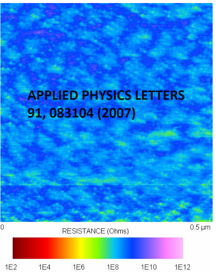
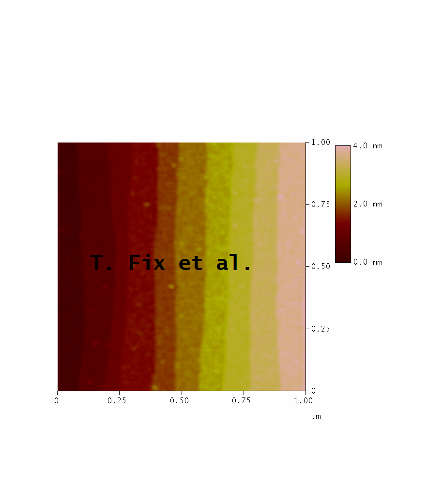
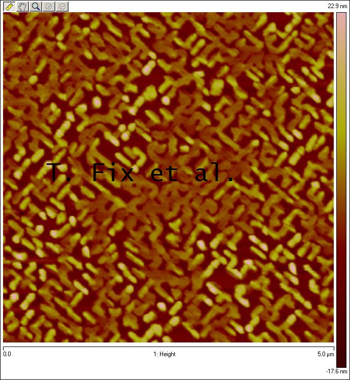
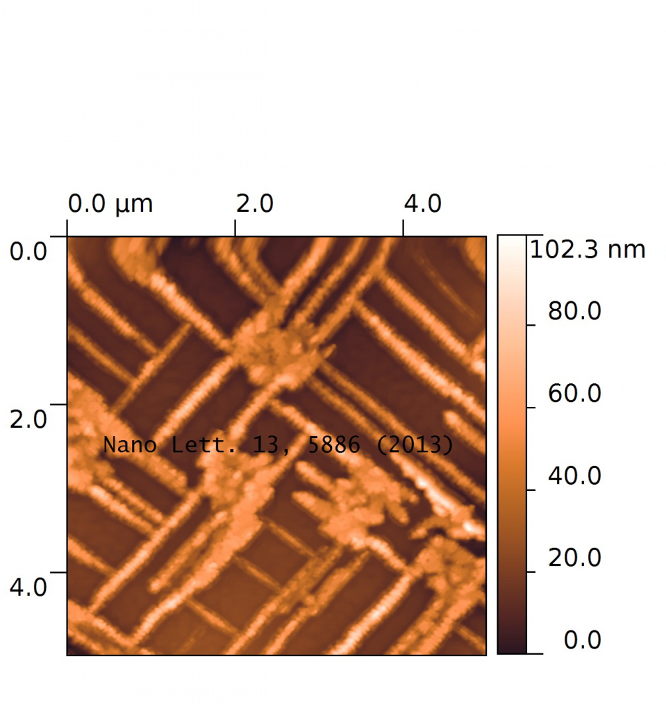
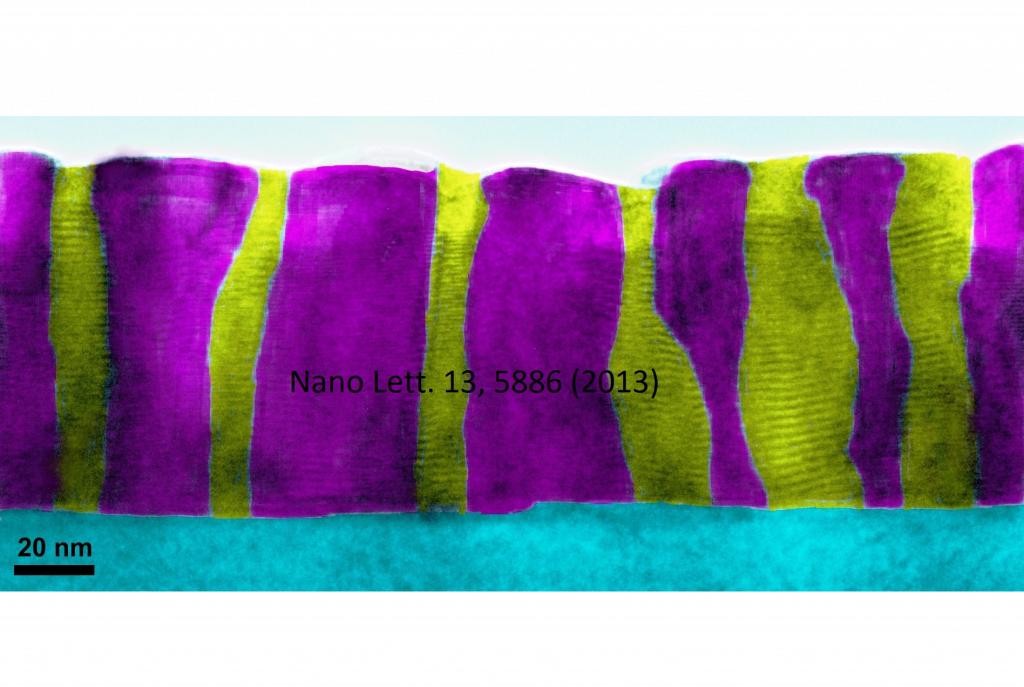
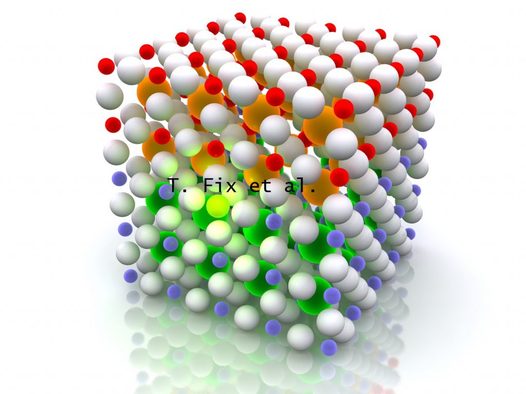
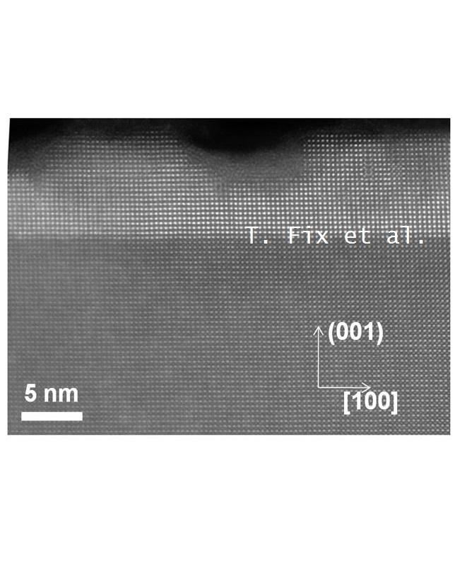
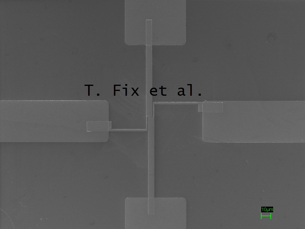
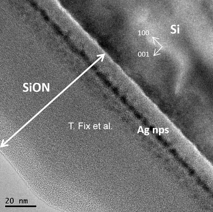
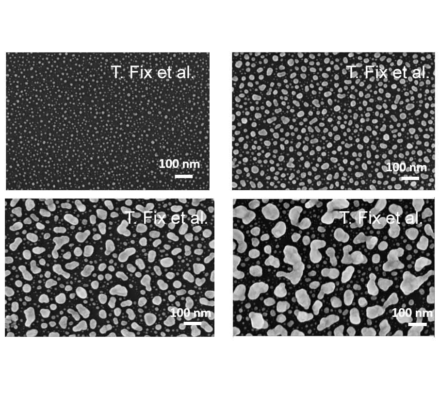
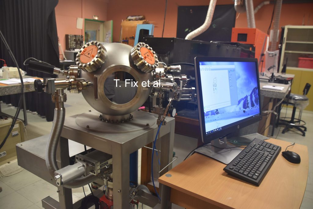
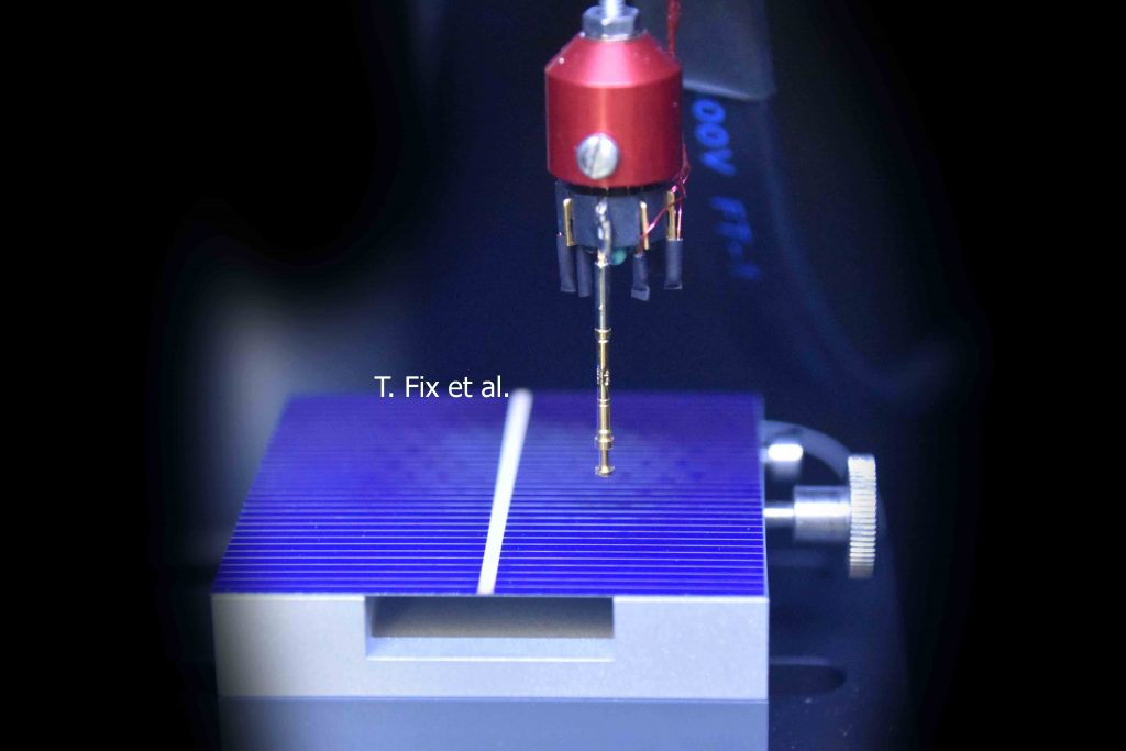
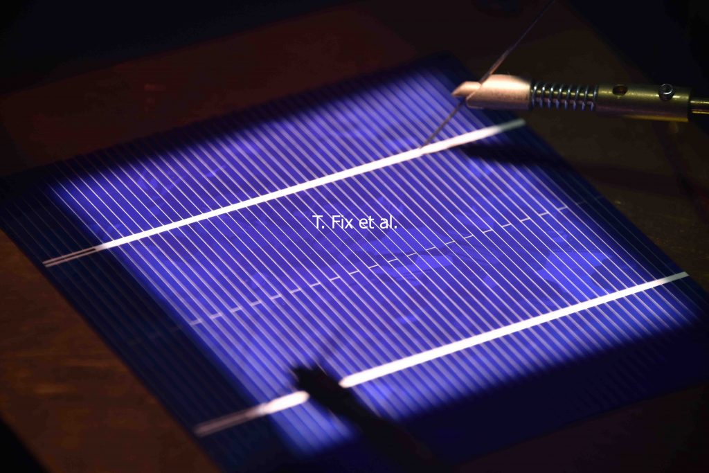
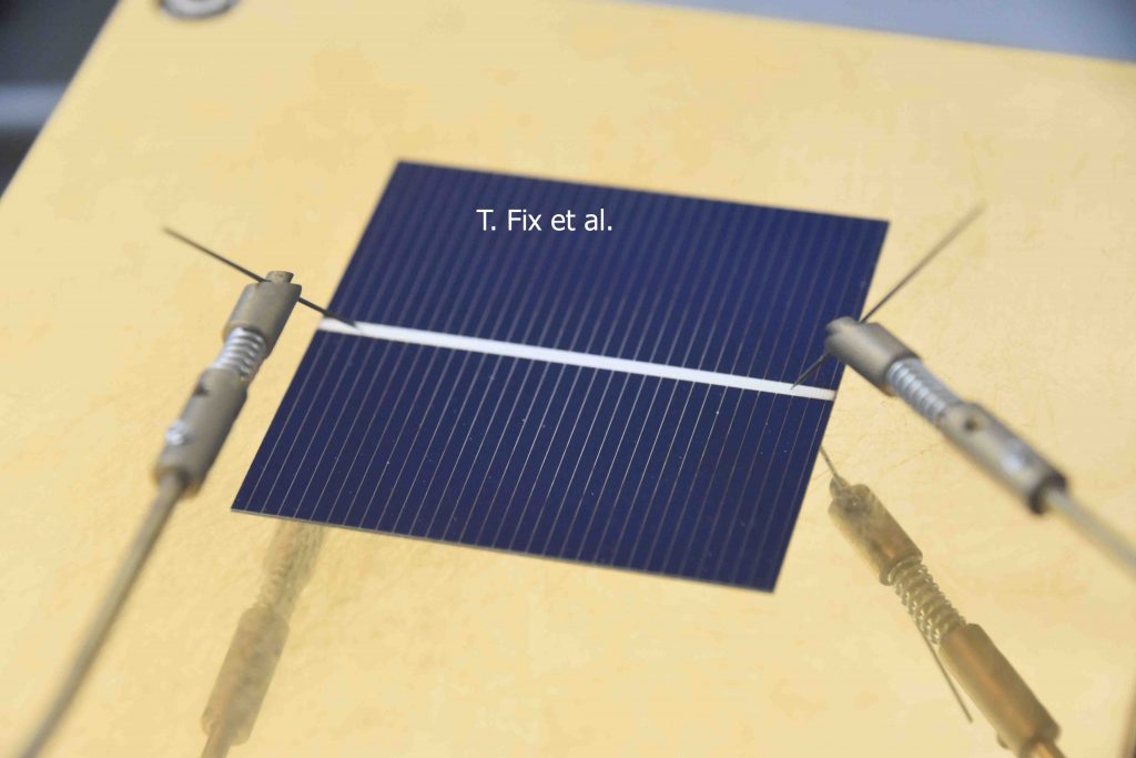
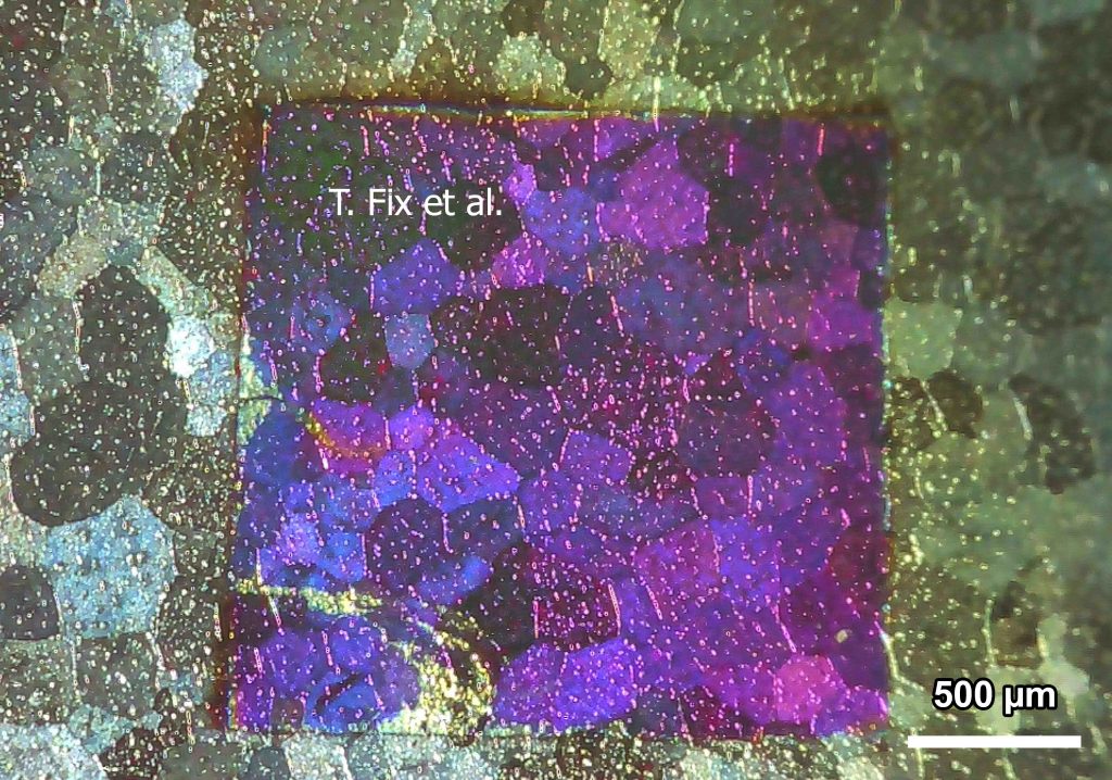
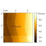
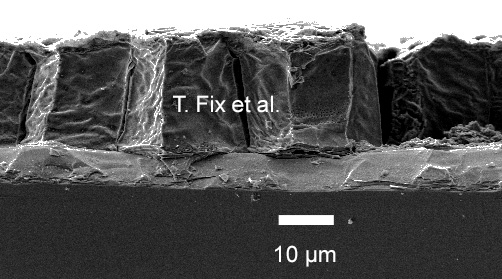
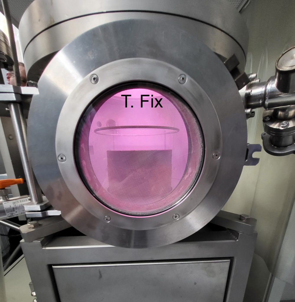
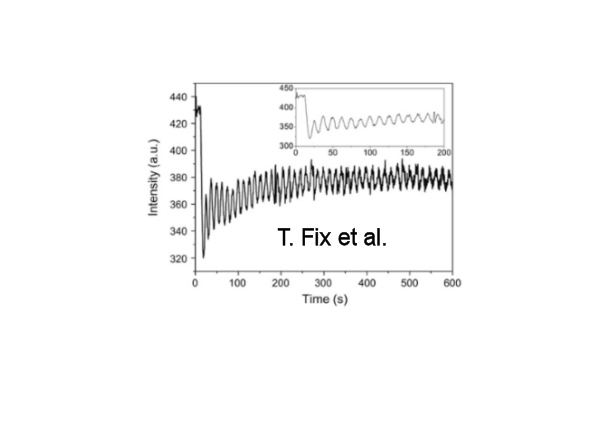
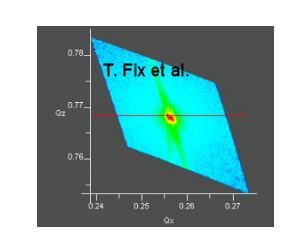
CTAFM resistance through a tunnel barrier (Lévy flights)Atomic steps of an oxide substrate (AFM)Atomic steps of an oxide substrate (AFM)Thin film oxide (AFM)Oxide nanocomposite (AFM)Self-assembled epitaxial vertically aligned structures of La2CoMnO6-ZnO (TEM)Two-dimensional electron gas at the interfaceCross-section of a LaAlO3/SrTiO3 interface (HRTEM)Electron lithography for spin-FETElectron lithography for spin-FETSelected area diffraction of SnTiO3 film (TEM)RHEED image of an epitaxial thin filmRHEED image of an epitaxial thin filmc-Si solar cell made in MaCEPVSt John’s college, CambridgeTaiwan SynchrotronUS boats with PV and windNanopatterned diode (FIB)Encapsulant functionalised with photon conversionPlasma during pulsed laser deposition (PLD)Ag nanoparticles implanted in SiONAg nanoparticles on SiONPulsed laser deposition (PLD) systemSi solar cell in scanning Kelvin ProbeSi solar cell in solar simulatorSi solar cell for IV measurementOxidized Cu2O solar cellAtomic steps of a SiC substrateSilicon clathrate film on SiliconHydrogenation process in the PECVDRHEED oscillations of Nb:STO on NGO(001)Reciprocal space map of BFO//NSTO(001)Thermal imaging of PLD chamber with heater at 800°C